Welcome to HongShuo.
We use cookies to HongShuo our website for you and to improve it continuously. By confirming the button "Accept" you agree to the use of cookies. Under "Configure" you can accept various cookie categories or confirm that no cookies should be set other than those required to use the HongShuo company website. For further information, please see our privacy policy.
Configure
Accept
Home > Products > Machine Vision Light > Machine Vision Imaging System > 2.5D Phase Deflectometry Line-Scan Programmable Stripe Light Source
2.5D Phase Deflectometry Line-Scan Programmable Stripe Light Source

2.5D Phase Deflectometry Line-Scan Programmable Stripe Light Source

Product Features

◆Ideal for inspection of large-area flat, highly reflective surfaces, micro-scale topographic protrusions and recesses, and general surface defects.

◆Customizable length: maximum achievable length up to 2000 mm

◆Ultra-high precision: adjustable in 0.1 μs increments

◆Supports a maximum line rate of 100 kHz

Application scope

◆ Fold creases and micro-scratches on flexible OLED displays

◆ Surface quality of TGV (Through Glass Via) vias

◆ Inspection of surface pits, micro-protrusions, and micro-scratches on aluminum battery cans and top covers, as well as weld seam quality

◆ Highly reflective surface defects encountered on semiconductor wafers and throughout the semiconductor packaging process

high-end manufacturing, micron-scale defect inspection on surfaces that are highly reflective, transparent, or covered in complex background textures has long been a fundamental challenge for traditional 2D machine vision systems. Our 2.5D Phase Deflectometry Line-Scan Programmable Stripe Light Source is purpose-built to solve this persistent industry challenge. By projecting precision calibrated phase fringe patterns, it accurately captures micro-scale topographic variations on object surfaces—upgrading inspection capability from intensity-based imaging to depth-resolved imaging. It delivers high-efficiency, high-precision 2.5D defect detection solutions for lithium battery, 3C electronics, glass panel, and semiconductor manufacturing sectors.


Working Principle

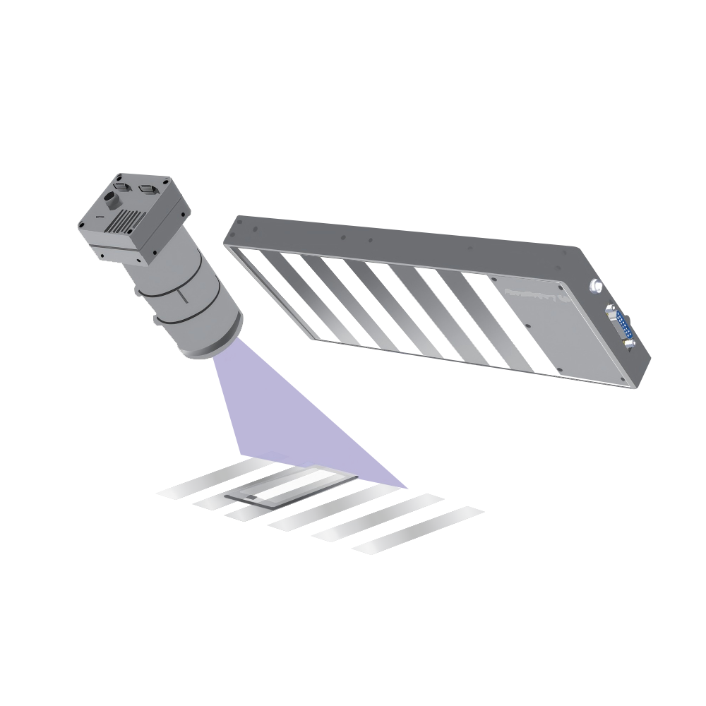
Phase Measuring Deflectometry (PMD) combines structured light projection and phase-based reconstruction at its core.

  1. Fringe Projection: The light source projects a sequence of high-contrast, sinusoidal fringe patterns with known phase values onto the target object surface.
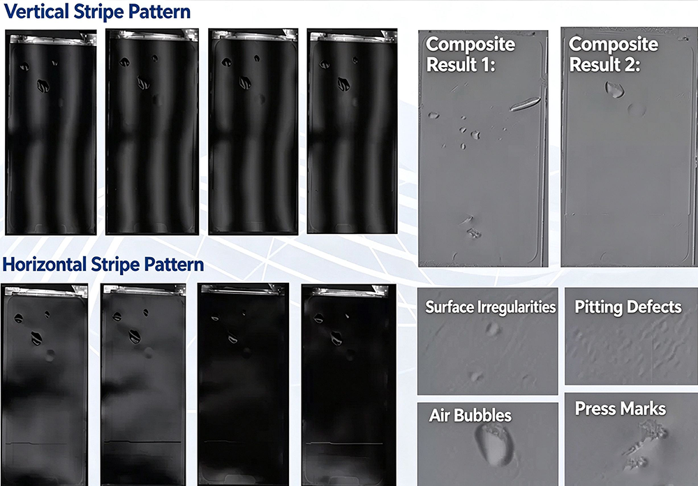
  2. Deformation Capture: A synchronized line-scan camera captures fringe images deformed by the local surface curvature of the object. Microscopic protrusions, recesses, and scratches on the surface produce corresponding measurable phase shifts in the projected fringe pattern.
  3. Phase Reconstruction: High-precision on-board processing solves for phase values across every pixel by analyzing a sequence of acquired phase-shifted fringe images.
  4. Topography Reconstruction: Phase values are converted to height measurements to generate a 2.5D micro-topographic profile of the object surface, clearly and quantitatively visualizing all target defects.

Core Advantages

  1. Overcome high-reflectivity material inspection limitations

  2. Pain point: Conventional light sources produce harsh glare and halation when aimed at mirror-finish, polished metal, or glass surfaces, obscuring true defects and leading to high rates of false rejection and missed defects.
  3. Our solution: PMD does not rely on surface grayscale or color information. Instead, it perceives local surface gradients by parsing fringe phase shifts. This built-in capability suppresses specular reflection interference, enabling reliable identification of micron-scale topographic defects including scratches, pits, and edge chipping.

  4. Eliminate complex background texture interference
  5. Pain point: When workpieces carry inherent surface textures such as brushed grain, matte finishing, or printed markings, these background features severely obscure defect recognition.
  6. Our solution: The system extracts features with measurable depth variation from the reconstructed shape map, effectively filtering out background patterns that show no height change. It reliably separates true defects from background on parts ranging from brushed aluminum housings to blue-film coated battery cells.

  7. Single-scan, multi-defect composite inspection
  8. Pain point: Traditional setups require multiple workstations and separate light sources to simultaneously inspect topographic defects, surface contamination, and other visual flaws, leading to low production efficiency.
  9. Our solution: A single scan generates multiple parallel algorithm outputs, including a shape map highlighting height variations and a gloss ratio map reflecting surface reflectance differences. One integrated system can simultaneously verify topographic defects (protrusions, scratches) and cosmetic defects (contamination, uneven oxidation), significantly reducing required inspection cycle time.

  10. Purpose-built for high-speed production lines
  11. Pain point: High-precision inspection historically requires tradeoffs in speed, failing to meet the throughput demands of modern manufacturing lines.
  12. Our solution: Integrated high-speed strobing supports a maximum projection frequency of 200 kHz. When paired with the parallel processing logic of line-scan cameras, it synchronizes image acquisition and 2.5D data fusion, delivering stable, high-efficiency inline inspection even for high-speed dynamic production environments.

Typical Applications

  1. 3C Electronics: Scratch and pit inspection for phone mid-frames, backplates, and heat sinks; surface defect inspection for laptop computer housings.
  2. New Energy Manufacturing: Bubble and contamination inspection on blue-film battery surfaces; flatness and defect inspection on battery tabs and aluminum cell cans.
  3. Glass Panel Manufacturing: Edge chipping, pitting, and scratch inspection for phone cover glass, in-vehicle displays, and tempered protective films.
  4. Semiconductor Manufacturing: Polishing defects and micro-defect inspection on bare wafers and chip package surfaces.

Illumination Safety
2.5D Phase Deflectometry Illumination Case Images
How Can we help?
Please send us your message. We will contact you as soon as possible..
Contact Us
* Name
Phone
* Email
* Message