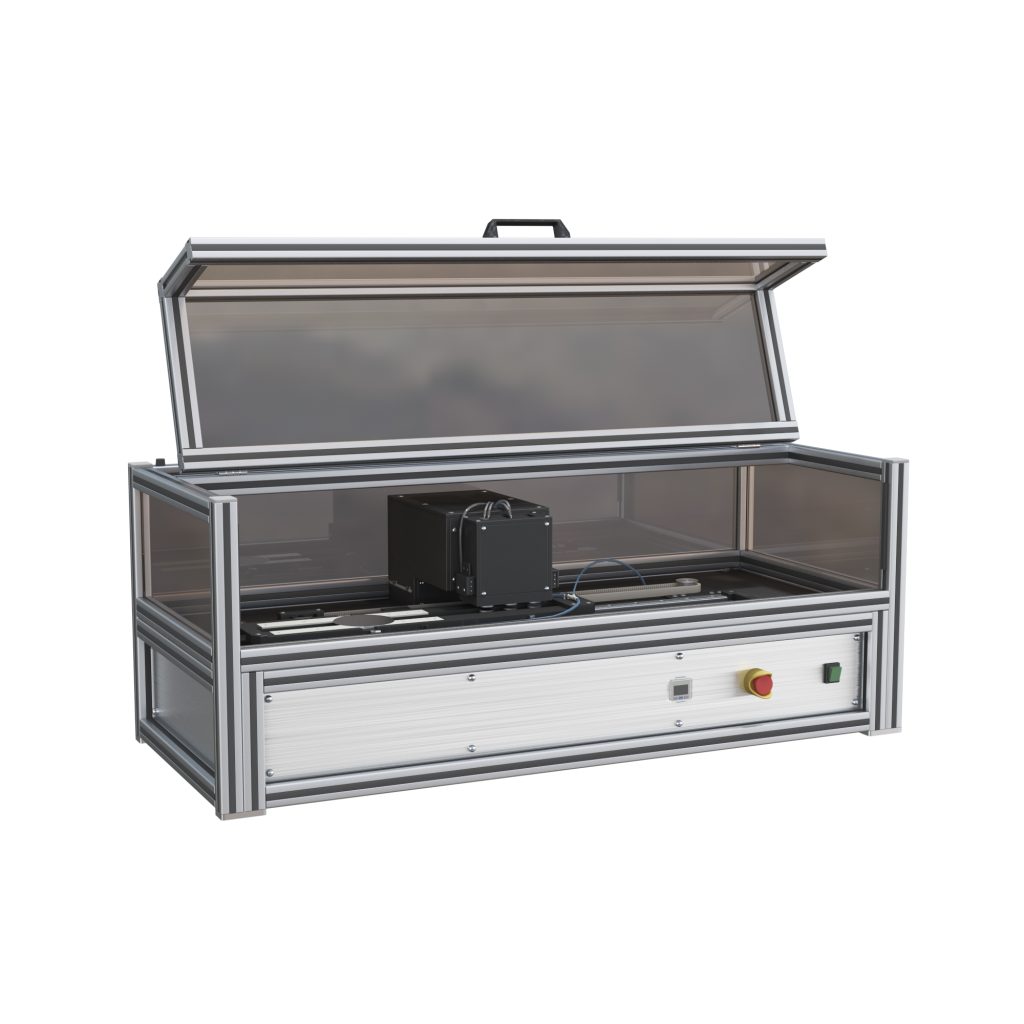
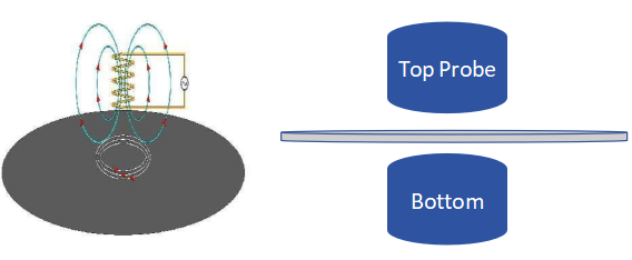
◆non-contact eddy-current probes
◆Non-Damage measurement by non-contact measurement
◆Fast testing speed
◆Good repeatability
◆High test sensitivity
◆ Semiconductor material
◆ Graphene
◆ Transparent conductive film
◆ Carbon Nanotubes
◆ Metal
Parameters | Probe | Resistance Range | Resistance Range | Testing Method |
---|---|---|---|---|
Range | Low-resistance probe | 0.005-1 Ω/sq | 0.25-50 mΩ·cm | Eddy current method, non- contact |
Mid-resistance probe | 0.05-10 Ω/sq | 2.5-500 mΩ·cm | ||
High-resistance probe | 10-3000 Ω/sq | 0.5-150 Ω·cm | ||
Ingot probe | 0.01-2 Ω·cm | |||
Repeatability | <0.2%(≤50% range) | <0.5%(>50% range) | ||
Accuracy | <2%(≤50% range) | <3%(>50% range) | ||
Probe Information | Type of Probe: Dual-probe (upper and lower probes with a 2-3mm gap), Probe Diameter: Outer diameter 20mm, Inner diameter 14mm (effective testing part), Probe Gap: 30mm | |||
Coordinate Settings | Arbitrary Coordinate Settings | |||
Store data | Internal Database Storage (Exportable Table Files), PDF Test Report containing test information (time, operator), wafer information (number, size, thickness), data information (number of test points, max/min/average values, relative standard deviation, etc.), contour maps, surface maps, etc. CSV Table Data Storable to Remote Server Modifiable report information as per customer requirements | |||
WAFER Information | Size: 2”-8” (inches) | Thickness:100-1500mm | ||
System Requirements | Power Supply: AC220V,50/60Hz Relative Humidity:20%-80%RH | Power: 600W Environment: Temperature 24℃±10℃ Size: 975*465*425(mm) Lifespan: >10 years |
Material | Resistivity | Sheet Resistance |
---|---|---|
Silicon wafer | Y | Y |
Sic wafer /Ingot | Y | Y |
GaO wafer /Ingot | Y | Y |
GaN wafer 2DEGI | Y | Y |
GaAs 2EDG | N | Y |
GZO/LTPS/ITO | N | Y |
flat panel) | N | Y |
TCO(Touch panel) | N | Y |
Graphene | N | Y |
Metal film | N | Y |