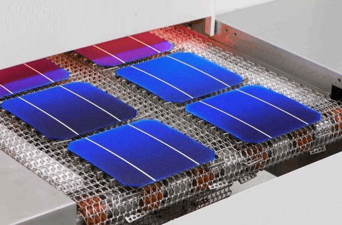
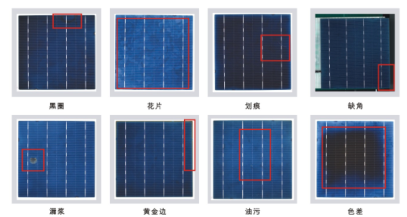
The solar silicon wafer visual inspection system fully automates the detection and measurement process, avoiding human intervention, and achieving an efficient, highly repetitive, and highly reliable detection and measurement process.
Widely used in the production line of solar silicon wafers, it ensures that every defective solar silicon wafer does not flow into the next production process without affecting the production capacity of the production line.
Solar silicon wafer visual inspection, silicon wafer appearance defect detection plan - machine vision_ Visual inspection equipment_ 3D Vision_ defect detection
Technical characteristics of solar silicon wafer visual inspection system
High detection accuracy and precise detection of defects
The detection accuracy is as high as 0.02mm, which can detect very fine defects.
There are many types of color sorting, up to 24 types
According to the color difference of silicon wafers, 24 kinds of color difference are classified.


