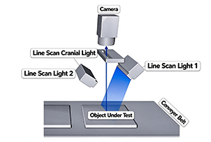
◆ Silicon wafer surface inspection for scratches, pinholes, pits, edge chipping, particles, and oxide layer defects
◆ Chip surface inspection for dents, gold pad scratches, carrier micro-pits, and circuit protrusion/recess defects
◆ Ceramic substrate surface inspection for micro-holes, scratches, warpage, and chipping
◆ Glass surface inspection for micron-level scratches, pitting, edge chipping, contamination, and coating flaws
◆ Coating layer pinhole, surface pit, and grinding mark defect identification
◆ Micro-indentations and concave/convex defects on glass substrates and metal electrode surfaces
◆ Polished flat surfaces of stainless steel and aluminum alloy, identifying fine scratches, dents, impact marks, and concave/convex defects on brushed surfaces (normal brushing texture can be filtered out)
◆ PCB gold finger scratches, copper surface pits, protrusions, pinholes, and dent defects